- 您现在的位置:买卖IC网 > Sheet目录2004 > LTC1659IMS8#TRPBF (Linear Technology)IC DAC 12BIT R-R 8-MSOP
LTC1659
6
1659fa
PIN FUNCTIONS
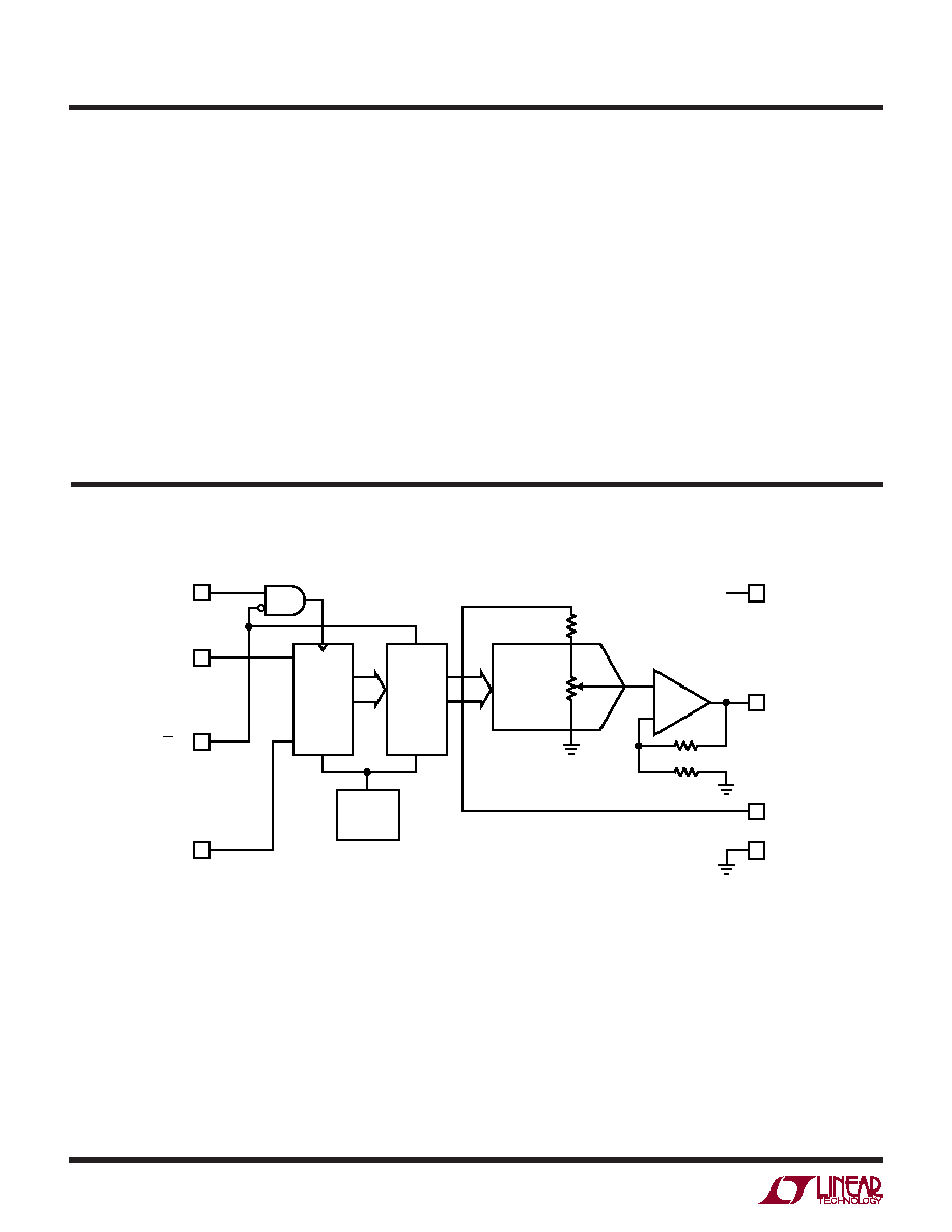
BLOCK DIAGRAM
CLK (Pin 1): Serial Interface Clock. Internal Schmitt trigger
on this input allows direct optocoupler interface.
DIN (Pin 2): Serial Interface Data. Data on the DIN pin is
latched into the shift register on the rising edge of the
serial clock.
CS/LD (Pin 3): Serial Interface Enable and Load Control.
When
CS/LD is low the CLK signal is enabled, so the data
can be clocked in. When
CS/LDispulledhigh,dataisloaded
from the shift register into the DAC register, updating the
DAC output and the CLK is disabled internally.
DOUT (Pin 4): Output of the Shift Register which Becomes
Valid on the Rising Edge of the Serial Clock.
GND (Pin 5): Ground.
REF (Pin 6): Reference Input. This pin can be tied to VCC.
The output will swing from 0V to REF. The typical input
resistance is 28k.
VOUT (Pin 7): Buffered DAC Output.
VCC (Pin 8): Positive Supply Input. 2.7V ≤ VCC ≤ 5.5V.
Requires a bypass capacitor to ground.
DAC
REGISTER
LD
12-BIT
SHIFT
REGISTER
POWER-ON
RESET
1659 BD
CLK 1
DIN 2
DOUT 4
VOUT
7
REF
6
GND
5
VCC
8
3
CS/LD
12-BIT
DAC
+
–
发布紧急采购,3分钟左右您将得到回复。
相关PDF资料
LTC1660IN
IC D/A CONV 10BIT OCTAL 16-DIP
LTC1661IMS8#TRPBF
IC D/A CONV 10BIT MICRPWR 8-MSOP
LTC1662IN8#PBF
IC D/A CONV 10BIT MICRPWR 8-DIP
LTC1663-1CS5#TRM
IC DAC 10BIT R-R TSOT23-5
LTC1664IN
IC DAC 10BIT QUAD MICRPWR 16DIP
LTC1667CG#PBF
IC D/A CONV 14BIT 50MSPS 28-SSOP
LTC1686IS8#TRPBF
IC TXRX RS485 PREC DELAY 8-SOIC
LTC1688IS
IC DVR 100MBPS RS485 QUAD 16SOIC
相关代理商/技术参数
LTC1659IS8
功能描述:IC D/A CONV 12BIT R-R 8-SOIC RoHS:否 类别:集成电路 (IC) >> 数据采集 - 数模转换器 系列:- 产品培训模块:LTC263x 12-, 10-, and 8-Bit VOUT DAC Family 特色产品:LTC2636 - Octal 12-/10-/8-Bit SPI VOUT DACs with 10ppm/°C Reference 标准包装:91 系列:- 设置时间:4µs 位数:10 数据接口:MICROWIRE?,串行,SPI? 转换器数目:8 电压电源:单电源 功率耗散(最大):2.7mW 工作温度:-40°C ~ 85°C 安装类型:表面贴装 封装/外壳:14-WFDFN 裸露焊盘 供应商设备封装:14-DFN-EP(4x3) 包装:管件 输出数目和类型:8 电压,单极 采样率(每秒):*
LTC1659IS8#PBF
功能描述:IC D/A CONV 12BIT R-R 8-SOIC RoHS:是 类别:集成电路 (IC) >> 数据采集 - 数模转换器 系列:- 产品培训模块:Lead (SnPb) Finish for COTS
Obsolescence Mitigation Program 标准包装:50 系列:- 设置时间:4µs 位数:12 数据接口:串行 转换器数目:2 电压电源:单电源 功率耗散(最大):- 工作温度:-40°C ~ 85°C 安装类型:表面贴装 封装/外壳:8-TSSOP,8-MSOP(0.118",3.00mm 宽) 供应商设备封装:8-uMAX 包装:管件 输出数目和类型:2 电压,单极 采样率(每秒):* 产品目录页面:1398 (CN2011-ZH PDF)
LTC1659IS8#TR
功能描述:IC DAC 12BIT R-R MICROPWR 8SOIC RoHS:否 类别:集成电路 (IC) >> 数据采集 - 数模转换器 系列:- 产品培训模块:LTC263x 12-, 10-, and 8-Bit VOUT DAC Family 特色产品:LTC2636 - Octal 12-/10-/8-Bit SPI VOUT DACs with 10ppm/°C Reference 标准包装:91 系列:- 设置时间:4µs 位数:10 数据接口:MICROWIRE?,串行,SPI? 转换器数目:8 电压电源:单电源 功率耗散(最大):2.7mW 工作温度:-40°C ~ 85°C 安装类型:表面贴装 封装/外壳:14-WFDFN 裸露焊盘 供应商设备封装:14-DFN-EP(4x3) 包装:管件 输出数目和类型:8 电压,单极 采样率(每秒):*
LTC1659IS8#TRPBF
功能描述:IC D/A CONV 12BIT R-R 8-SOIC RoHS:是 类别:集成电路 (IC) >> 数据采集 - 数模转换器 系列:- 产品培训模块:LTC263x 12-, 10-, and 8-Bit VOUT DAC Family 特色产品:LTC2636 - Octal 12-/10-/8-Bit SPI VOUT DACs with 10ppm/°C Reference 标准包装:91 系列:- 设置时间:4µs 位数:10 数据接口:MICROWIRE?,串行,SPI? 转换器数目:8 电压电源:单电源 功率耗散(最大):2.7mW 工作温度:-40°C ~ 85°C 安装类型:表面贴装 封装/外壳:14-WFDFN 裸露焊盘 供应商设备封装:14-DFN-EP(4x3) 包装:管件 输出数目和类型:8 电压,单极 采样率(每秒):*
LTC1660CGN
功能描述:IC D/A CONV 10BIT OCTAL 16-SSOP RoHS:否 类别:集成电路 (IC) >> 数据采集 - 数模转换器 系列:- 标准包装:47 系列:- 设置时间:2µs 位数:14 数据接口:并联 转换器数目:1 电压电源:单电源 功率耗散(最大):55µW 工作温度:-40°C ~ 85°C 安装类型:表面贴装 封装/外壳:28-SSOP(0.209",5.30mm 宽) 供应商设备封装:28-SSOP 包装:管件 输出数目和类型:1 电流,单极;1 电流,双极 采样率(每秒):*
LTC1660CGN#PBF
功能描述:IC D/A CONV 10BIT OCTAL 16-SSOP RoHS:是 类别:集成电路 (IC) >> 数据采集 - 数模转换器 系列:- 产品培训模块:Lead (SnPb) Finish for COTS
Obsolescence Mitigation Program 标准包装:50 系列:- 设置时间:4µs 位数:12 数据接口:串行 转换器数目:2 电压电源:单电源 功率耗散(最大):- 工作温度:-40°C ~ 85°C 安装类型:表面贴装 封装/外壳:8-TSSOP,8-MSOP(0.118",3.00mm 宽) 供应商设备封装:8-uMAX 包装:管件 输出数目和类型:2 电压,单极 采样率(每秒):* 产品目录页面:1398 (CN2011-ZH PDF)
LTC1660CGN#PBF
制造商:Linear Technology 功能描述:IC D/A CONVERTER OCTAL 10-BIT CMOS
LTC1660CGN#TR
功能描述:IC DAC 10BIT OCTAL MCRPWR 16SSOP RoHS:否 类别:集成电路 (IC) >> 数据采集 - 数模转换器 系列:- 标准包装:47 系列:- 设置时间:2µs 位数:14 数据接口:并联 转换器数目:1 电压电源:单电源 功率耗散(最大):55µW 工作温度:-40°C ~ 85°C 安装类型:表面贴装 封装/外壳:28-SSOP(0.209",5.30mm 宽) 供应商设备封装:28-SSOP 包装:管件 输出数目和类型:1 电流,单极;1 电流,双极 采样率(每秒):*